 The
TLC2543 has an SPI interface, which will be connected to four BASIC
Stamp pins and using the SHIFTOUT and SHIFTIN commands. The TLC2543 has
four control lines that concern us.
The
TLC2543 has an SPI interface, which will be connected to four BASIC
Stamp pins and using the SHIFTOUT and SHIFTIN commands. The TLC2543 has
four control lines that concern us.
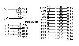
BASIC Stamp (OWL2) to TLC2543
analog to digital converter
The TLC2543 is the analog to digital converter EME Systems uses in the OWL2 series data logger. Many of the sensor data processing programs described on this web site call this (or similar) ADread routine to get their data.
The TLC2543 is an advanced analog to digital converter chip from Texas Instruments, and it uses their proprietary switched capacitor technology to achieve high accuracy. Please refer to the TLC2543 data sheet for detailed information. It has eleven voltage inputs. The resolution is 12 bits, so there are 4096 steps dividing the voltage range from (ref-) to (ref+). The chip requires an external reference for (ref-) and (ref+). If the reference is 4.096 volts, then the result from the ADC will read directly in millivolts. If the reference is 5.000 volts, it will read 4096 increments of 1.2207 millivolts per bit. A reference of 5.12 volts would be read 4096 increments of 1.25 millivolts. The demo routine below assumes a 5 volts reference and shows the math to convert the reading into even units of millivolts, or into temperature, as it might do for an LM34 temperature sensor that generates 10 millivolts per degree Fahrenheit.
The chip is quite robust. A resistor of around 330 ohms can be added in front of each input to protect it from ESD and mis-wiring. These are shown in the schematic diagram as protection between the inputs and the outside world. Additional input protection involving diode clamps can improve the level of protection.
The
TLC2543 has an SPI interface, which will be connected to four BASIC
Stamp pins and using the SHIFTOUT and SHIFTIN commands. The TLC2543 has
four control lines that concern us.
The OWL2pe data logger from EME Systems uses a precision 4.096 volt reference, with respect to common, so the analog input range is zero to 4.096 volts at one millivolt per bit. It talks to the TLC2543 on AUXIO pins x0, x1, x2 and x14. And it brings nine of the TLC2543 inputs to the edge of the module for applications, and uses two of them internally for monitoring the Vin power supply voltage and the internal board temperature.
The following program runs a demo, to scan 11 input channels, convert the count to millivolts, and to display the result on the debug screen. Note that this program names the sdi and sdo from the reference point of the BASIC Stamp. The sdo output from the Stamp connects to the sdi input of the TLC2543 and the complement, Stamp sdi to TLC2543 sdo.
'{PBASIC 2.5}
' ADread subroutine.
' On command, returns 12 bit digital data from one of 11 analog channels.
' The value of ADch from 0 to 10 selects external analog inputs.
' ADch=14 puts the converter into its sleep mode.
' converter has 5 volt reference, connection to the Vdd power supply, for 1.2207 mV per bit

sclk PIN 15 ' clock out from BS2 to AD2543
sdo PIN 14 ' data out from BS2 to AD2543 sdi
sdi PIN 13 ' data in from AD2543 sdo to BS2
ADcs PIN 12 ' AD2543 chip select, active low

ADch VAR Nib ' selects AD external channel 0-10
result VAR Word ' result, 12 bit A/D conversion

demo: ' to show off the subroutine below.
DIRS=$FFFF ' makes all Stamp pins outputs to start
OUTS=$1000 ' makes all pins except ADC chip select low to start
DO
 GOSUB ADwake ' makes a dummy conversion to initialize converter
 FOR ADch =0 TO 10 ' specify one of 11 input channels
 GOSUB ADread ' get millivolt data from that channel
 result = 14464 ** result + result ' convert count to millivolts.
 DEBUG DEC ADch,": ",DEC result,REP 32\5,cr ' display, use extra spaces to clear garbage
 NEXT
 GOSUB ADsleep
 NAP 7
 DEBUG home ' repeat the demo
LOOP

ADread: ' entry point to give result as count from 0 to 4095
 LOW ADcs ' select chip
 SHIFTOUT sdo,sclk,msbfirst,[ADch<<8\12] ' mode, left justify ADch
 SHIFTIN sdi,sclk,msbpre,[result\12] ' get result, 12 bits
 HIGH ADcs ' deselect chip
RETURN

ADsleep: ' entry point to put TLC2543 to sleep
 LOW ADcs ' select chip
 SHIFTOUT sdo,sclk,msbfirst,[$e\4] ' command=$e
 HIGH ADcs ' deselect chip
 LOW sdi ' keep this pin from floating in sleep
RETURN

ADwake:
 ADch=$b
 GOTO ADread
In this situation the scale
factor is 1.2207 millivolts per bit. The count value from 0
to 4095 returned by the TLC2543 has to be multiplied times that scale
factor to convert to volts. In Stampese, one way to do this
uses the ** operator as follows:
result = 14464 ** result + result ' convert count to millivolts.
The factor 14464 comes from the
fact that 14464/65536 is a close approximation to the decimal fraction
0.2207. The ** operator internally multiplies times 14464
(to 32 bits of precision) and then implicitly divides that product by
65536. Adding in result again makes the overall
multiplication time 1.2207. More details on this
magic on the math pages.
If the reference voltage is 4.096 volts, there will be no conversion necessary from counts to volts (assuming that the reference itself is right on accurate!). With a 5.120 volt reference, the operation result = result */320 can be used to convert from counts to millivolts as the scale factor is 1.25 millivolts per count. Note that 320/256 is equal to 1.25, and the division by 256 is implied in the Stamp */ operator.
A note about the ADwake
subroutine. To wake up the chip, send a
command to address any channel lower than than channel 14. The first
reading returned will sometimes be in error, due to internal settling
delays, so throw it away. The same thing goes for the first reading
after the chip is powered up. Throw the first reading away
and take a
second one to get it right. Note that this program uses the
ADwake
routine at the top of the loop, where it will be executed prior to the
first time through the loop and also after each NAP. Note
that to achieve minimum battery current, the above program would also
have to attend to the other Stamp pins in an appropriate manner.
The program assumes that those other Stamp pins are
uncommitted. The
ADwake routine addresses channle $b,an internal reference point at
Vrev/2, but it could just as well address any of the input channels.
Circuit layout makes a big difference with the performance of the
ADC. The reference must be stable, and there must not be ground
bounce in series with the analog or reference inputs, and the power
supply must be stable and well bypassed.
If a device connected to an
input has high source resistance or if you need lowpass filtering on an
input, it is possible to hang a capacitor, say 0.33 microfarad, on the
analog input pin, but there are issues to consider. An
explanation of how the TLC2543 works inside will clarify this.
When a channel is addressed, a 60 picofarad
capacitor in series with a 1kohm resistor (approximate model internal
to the TLC2543!) is connected to that input channel abruptly
just after the address is decoded, that is, after the first four bits
of the SHIFTOUT command from the Stamp. Then that input is
"sampled" during the last 8 clock pulses of the SHIFTOUT.
After that, the sample is held while the actual conversion
takes place. The "sampling" period is determined by
the SHIFTOUT clock rate of around 16 kilohertz (BS2). So the
sampling period is around 0.0005 second (0.005 = 8 * 1/16000).
The voltage transfered to that 60 pf capacitor inside the
TLC2543 at the end of that interval should equal the input voltage you
want to measure, within one part in 4096. For example, the
time constant of 60 pf with 1 megaohm of input resistance is
0.00006 second, which is only 10 times less than the sampling
period, so it would not settle completely. It is better to
keep the input resistance below 10k ohms so that the input has time to
settle to the correct value within the 0.0005 seconds. There
are other reasons too, to keep the input resistance below 10kohms, one
being leakage between the channels. The sampling
interval is relatively long due to the slow clock speed of the BASIC
Stamp. The faster Stamps would require a correspondingly
lower input source resistance, because they have a faster SHIFTOUT
clock. Now suppose a 0.3 uf capacitor charged to some
voltage is hung on the input. When that is
connected abruptly to a 60pf capacitor inside the TLC2543, the charge
will be distributed in the ratio of the two capacitors, which is
0.0002. (0.0002 = 60E-6 / 0.3). That
could mean up to a 1 millivolt worst case change in the voltage sampled
at the input, which is the same order of magnitude as the resolution of
the ADC. A larger capacitor would not shift as
much due to being connected to the 60pf sampling capacitor, but
remember that the capacitor has to be recharged to the correct voltage
before the channel is sampled again. I hope that clarifies
the considerations that go into filtering and input source impedance.
One symptom of too high an
input source resistance or a bad RC time constant at the input, is that
the reading on one channel appears to affect the reading on a
neighboring channel. Remember though that channels that are
not connected to anything at all will still give readings, and those
readings will tend to drift toward the readings on neighboring
channels. Do not connect the inputs to voltages
more than 0.3 volt below Vss or above Vdd, as this will lead to bad
readings on all the channels, not only the one that has the excess
voltage input. If excess voltages might be present in a
system, use diode clamps or other means to limit the voltage seen at
the converter inputs.
The actual conversion is done by the TLC2543 using an internal high speed conversion clock, and takes only about 10 microseconds maximum. That is much less than the time it takes for the Stamp to get ready to read out the data using its SHIFTIN command. Inside the TLC2543, it uses switched capacitor technology to redistribute the charge acquired by the 60 pf input capacitor, in a clever successive approximation scheme that is explained in the TI data sheet.